How to prepare PCB CAM files in EAGLE
0. Draw the board
So that you have something to send to the board house.
1. DRC: Design Rule Check
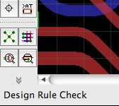
Locate and run Design Rule Check. A dialog with a lot of design constraint parameters will open. You need to check with your board house to know the exact values they allow. You should then enter them here and never deviate.
1.1 DRC![]()
![]() clearance
clearance

The most important parameters: trace clearance, pad clearance and via clearance. Typical values for a low-end board house would be 8mil or 0.2mm.
1.2 DRC Distance
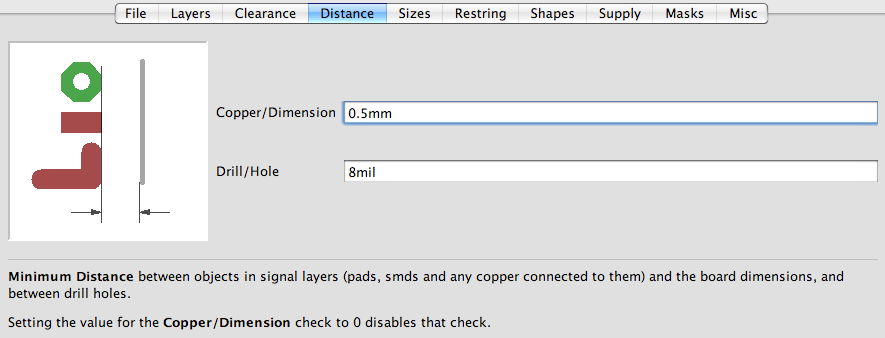
This is how far the edge of the PCB is from the copper. Don't put traces closer to the edge than this value. Normally about 0.5mm.
1.3 DRC Masks
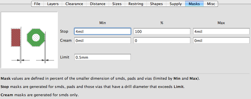
Stop: how far away from the edge of a SMD/pad the mask will be. If you're reading this you don't need Cream.
Limit is an interesting parameter. It allows to specify the size of pads/vias that do not need to be automatically unmasked. Anything smaller than Limit will be covered with solder mask. Useful for vias. If you need some vias open, it can be done individually in the properties dialog, or by drawing polygons in tStop/bStop layers.
1.4 DRC Must Pass
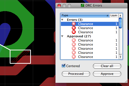
Some DRC errors can't be avoided because of package specifics. If it is certain that this particular DRC error can be allowed, Approve it. It will be added to the list of approved errors and will not bother you again. Other problems should be corrected.
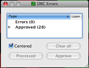
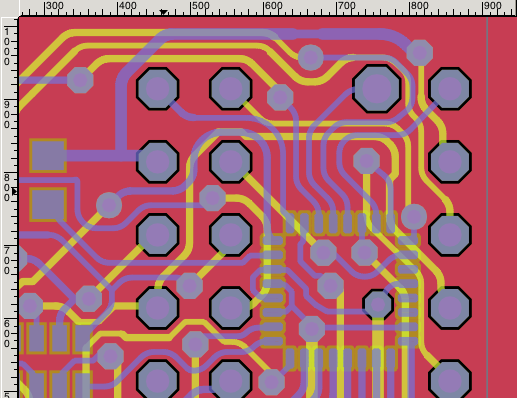
When you get a picture like this, this is good. Time to make the drill and plotting files.
2. CAM Processor
CAM Processor processes CAM files.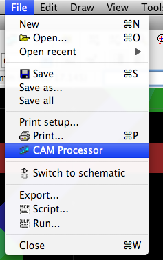
CAM processor transforms the contents of one or several layers into various file formats. To make several files, a Job with several tasks can be created. Fortunately, the most typical Jobs are already defined and packaged with EAGLE. They can be found in cam/ folder wherever your EAGLE is installed.
2.1 Drill Files
Open a standard Job called "excellon.cam": Open -> Job... -> excellon.camIt's probably a good idea to make sure that output paths for the job are convenient. By default they will generate files in the project folder and project folder probably already contains a lot of files.
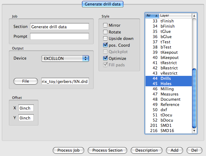
Run: Process Job! and there are .dri and .drd files on your disk now.
2.2 Photoplotter Philes
Now on to the Gerbers. Modern gerber files are in fact called GERBER 274X. File -> Open -> gerb274x.cam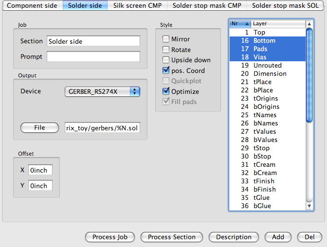
This job is comprised of several sections. The title of each section is listed in the tabs at the top of the dialog. Verbatim: component side (red, Top), solder side (blue, Bottom), Silkscreen (top), Solder Mask (top), Solder Mask (bottom). Everything is prepared already, although you might want to uncheck "Mirror" for the bottom layers, depending.
3. Results Check
3.1 Install gerbv
There is a good, free, opensource and everything viewer for gerb274x files: gerbv. It runs on all popular OS's, easy to use too. Get it here: http://gerbv.sf.net
3.2 Look At The Results
Go the the folder where you have all generated CAM-files and…$ gerbv * &
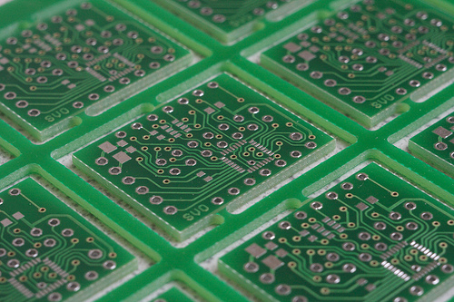
…check out the result. If everything looks realistic and causes no worries, it's time to zip them up together, write a letter with detailed description of what you expect to be done and send it to the board house. After a few days you're going to get the freshly manufactured boards:
That's about all there is to it.
—-—
Адрес этой статьи: https://caglrc.cc/gerberhowto/
Просьба указывать ссылку на первоисточник.
Copyright © 2009 Viacheslav Slavinsky svofski on gmail
Updated:
Thu Apr 9 20:25:56 MSD 2009