Zloshnik: vector CRT display based on 3ЛО1И
November, 5 2012At first I was going to build a CRT clock. But after learning that 3ЛО1И has a very short resource, about a thousand hours, I changed my mind. Zloshnik does not try to be a clock. Instead it's a decorative piece, something that you can fire up once in a while and enjoy its looks. It has a serial port which allows its usage as a vector terminal, but at the moment this function is not used.
Circuit description
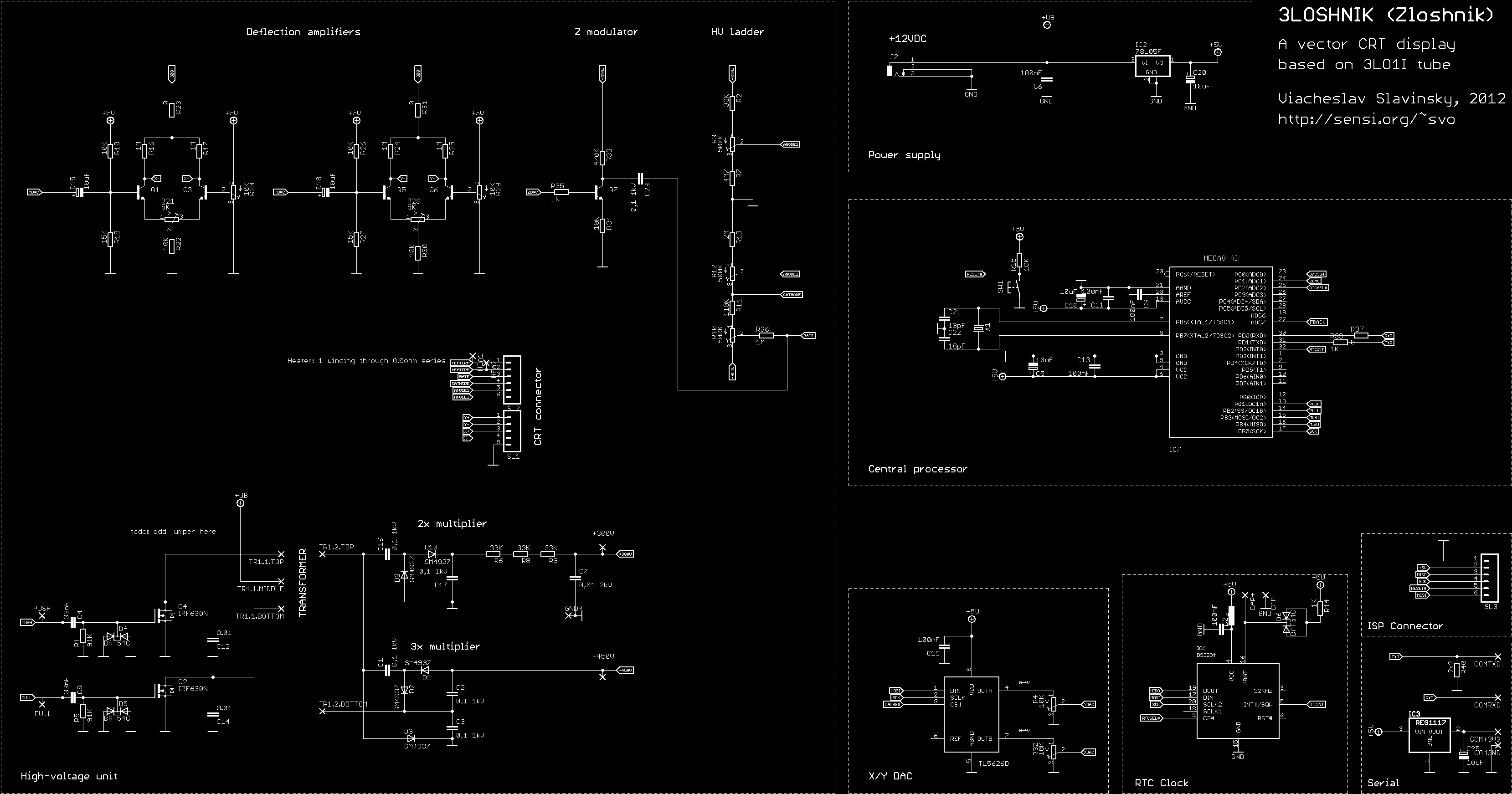
To power a CRT, even as small as this one, one needs pretty high voltages. To power a nixie clock 150-180 volts are enough, and this is easy to make with a boost converter. For 3LO1I the difference of potential between the cathode and the second anode has to be not less than 750 volts. This is why the power circuit differs significantly from that of a nixie clock. In a lot of homemade CRT projects the high voltages are produced using a power transformer from 220V, which makes them huge and heavy. For such a small tube I wanted to use a single source of +12VDC, which can be taken from any wall adapter.
The first part of voltage conversion is done with a push-pull cascade comprised by two MOSFETs IRF630N that drive a high-frequency transformer. The transformer is wound on a ferrite ring. The primary uses bifilar winding, 2×6 windings. Bifilar winding ensures high symmetry and it is important for a push-pull transformer circuit to work efficiently (or to work at all, since asymmetry here may kill the transistors). There is only one secondary, without a central tap. The quantity of windings on the secondary was found experimentally. With 12V input, there is approximately 150VAC on the secondary, or ±300Vp-p. There is another secondary with just one winding that provides power for the cathode heater. The heater must be floating without reference to the ground to avoid the potential difference between itself and the cathode. To avoid short circuit while the heater is cold, it is connected via a 0.5Ω resistor.
Long tail
The voltage from the secondary is doubled with a voltage doubler made with C16,D9,D10,C17 and smoothed with R6,R8,R9 и C7, which gives us +300V. Similarly, the tripler made with C1,D1,D2,D3,C2,C3 provides -450V. It is convenient to have voltages like so relative to the ground because this way we can use pretty common transistors with Uce=300V in the deflection system.
Between +300V and -450V there is a resistor ladder that provides all voltages needed to make a CRT work.
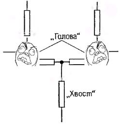
The deflection system is made with two differential pairs of the "long-tailed" kind, formed by transistors Q1,Q3 and Q5,Q6. Tune the amplifiers to make them really symmetric was the most fiddly part of the project. The blanking circuit is formed on transistor Q6. It allows to block the ray for a short period of time by changing the voltage on the grid. The deflection signals are formed by the DAC TL5626D. Blanking signal comes directly from the microcontroller.
The microcontroller ATmega8 does two important things. The first is to open and close the MOSFETs of the push-pull circuits. This is done by Timer1 and output compare unit OC1A/B and once set up does not require any attention. The other thing that occupies the controller is the formation of coordenates X,Y for the DAC and the blanking signal Z.
Zloshnik PCB
There's a wonderul PCB plugin called Teardrops, which makes vias teardrop-shaped
The PCB
The board did not fit into the 160x100 rectangle allowed by the free fersion of Eagle. Because of this I had to use other interesting tools to complete it. The process is like so: First the board (mostly complete) is converted into Specctra file. This file is then loaded into Freerouting, where the routing is completed and maybe optimized. Freerouting saves the result as a Specctra Session file, which can then be converted into a file for gEDA PCB, where the final touches are made and the board is printed. For this last conversion I wrote a python script, see files section. The file name is read_dsn.py.
I would not say that this process is very convenient, but I was pleased to learn that PCB is actually quite nice and not as bad as it appears at the first sight.
Parts raised above the board
I soldered the voltage multiplier parts a little bit raised from the PCB tracks to separate them a little bit. I don't know if it was worth it but it looks interesting.
Problems
The power circuit doesn't have any feedback and because of this it is sensitive to external factors. The power to heat the cathode is barely sufficient and thanks to this the process of initial heating can last some 10-20 minutes, during which the image moves significantly around the screen. The changes in ambient temperature also make the image travel across the screen, slowly.
Results
Contrary to the fears that the transformer will produce interference visible on the image, it wasn't observed at all. I think it can be explained partially by the toroidal construction of the transformer and partially by it's disposition near the tail of the tube, relatively far away from the deflection system. The resulting contraption turned out very compact and pretty. I turn it on every once in a while just to enjoy the green pictures formed by cathode rays. The image of a green CRT can't really be compared to anything among the modern screens. Unfortunately photographs can't really show all the magic of an analog screen.
The picture can be seen from behind of the screen
18:38
Circuits and source code
- The complete circuit[png]
- The PCB and the Python script [link]
- All Eagle files and C++ source code in the repo [link]
Useful links
- 3ЛО1И datasheet [istok2.com]
- 3LO1I on [tubehobby.com]
- Bifilar coil [wikipedia.org]
- Differential amplifier [wikipedia.org]
- Project log on the forum [avrfreaks.net], many details
- Transformers in switchmode power supplies [avrfreaks.net]
- Switch mode design [aplomb.nl]
- A collection of CRT clocks [webx.dk]
- Homemade scope probe with 3LO1I [remexpert.com]
- A very interesting thread about scope clocks on [elektroda.pl]
- A very detailed CRT clock project by Sascha Ittner [jogis-roehrenbunde.de]